On-board Computer System
The purpose of the on board computer for the AAUSAT-II pico-satellite is to supply sufficient computing power and storage for the data handling software and subsystem threads. It interfaces to other subsystem hardware via a CAN bus.
The OBC is based on an ARM7 processor with built-in CAN controller, the Atmel AT91SAM7A1.
- High speed 32 bit RISC CPU at 40MHz
- 2 MB static low-power RAM
- 4 MB Data storage (FLASH-RAM)
- 4 MB Code storage (FLASH-ROM)
- CAN bus interface @125kbps
- RS232 debugging/SW-upload interface
- Power monitor/power-on reset
- Full eCos/RedBoot support
- Run-time CPU speed selection (8/40 MHz)
- Low-power (<300mW @ 40MHz and <80mW @ 8MHz)
The code memory is a FLASH based chip that can be rewritten by setting a chip-select jumper on the board which makes the CPU execute the RedBoot boot loader which is resident in the lower area of the data FLASH chip. In this configuration, the code FLASH has chip-select 1 (CS1) and data FLASH has CS0. By removing jumper and rebooting the OBC the code FLASH has CS0 and data FLASH has CS1 which makes the OBC boot from the user application, i.e. the data handling software.
Current state and schedule
Current state:
- Engineering PC in operation
- Flight PCB done and tested
Next step:
- Flight readiness adaptations (e.g. conformal coating)
Documents
| Schematics | PDF file with schematics and PBC layout for the computer. The electrical and graphical design is intellectual property of Karl Kaas Laursen. |
Development Board
A development board has been produced so that teams from other subsystems can have a computer to use for implementing their OBC resident software. The main difference between the flight and development computer are the following features added to development:- two RS232 ports incl. transceiver.
- Eight general purpose I/O ports.
- ZIF socket for primary FLASH for external programming.
- No write protection for primary FLASH.
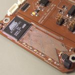
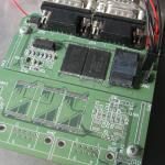
The first AAUOBC-IV prototype
On the left: Prototype OBC.
On the right: The OOPS-circuit enabling remotely controlled power-cycling from a PC.
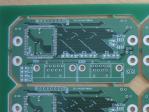
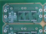
The new AAUOBC-IV development board
On the left: Top side PCB.
On the right: Bottom side PCB.
The AAUSAT-II Breakout Box
A breaout box has been built to ease the electrical interfacing of the EM and flight hardware. The Flight Preperation Panel of the spacecraft has two 10-pin connectors with connections to internal CAN bus, CMOS-level RS232 interface to OBC, battery charging, solar cell input and various RBF items.
The box translates the primitive electro-mechanical interface into standard connectors that allows easy connectivity with external computers, chargers and power supplies.
The picture shows the breakout box connected to the EM avionics stack (without the payload pcb).
Active Members
- Karl Kaas Laursen - System Engineer


